
42 Gb/mm2: Micron Doubles NAND Density for Late 2027 Chips
The company plans to use wafer bonding to boost speed and cut power usage in its next generation of storage.
By Lucia Orlov ·
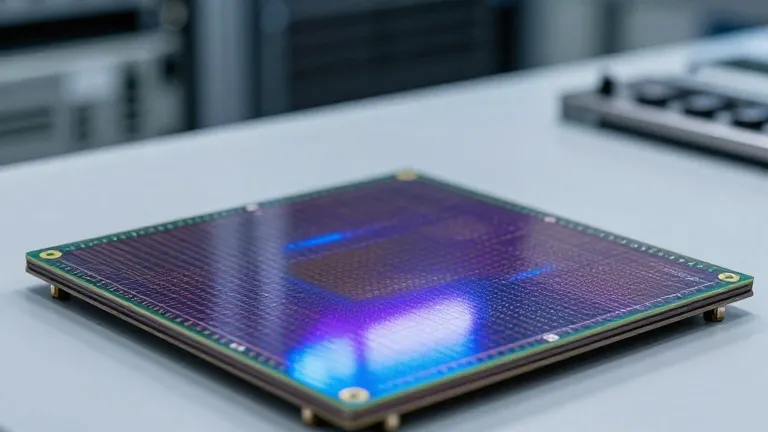
Micron Technology will begin ramping production of its G11 3D NAND flash in the second half of 2027. The new generation is designed to deliver double the storage density of the current standard while increasing input/output speeds and reducing power consumption.
The density increase is the most visible metric in the update. Micron expects G11 to reach approximately 42 Gb/mm2 in triple-level-cell form, up from about 21 Gb/mm2 in the existing G9 generation. This figure exceeds the next-generation NAND technologies currently planned by competitors Kioxia and Samsung, which are identified as BiCS10 and V10 respectively.
Performance metrics accompany the density gains. Micron projects I/O speeds will rise by up to 50 percent, moving from 3,600 MT/s to 5,400 MT/s. The company also states that the energy required to transfer each bit will drop by more than 25 percent. These improvements target conventional high-capacity SSDs for client and data center applications, as well as emerging storage devices built for artificial intelligence workloads that require high bandwidth and efficient power management.
The architectural shift relies on wafer-on-wafer bonding. This process allows Micron to manufacture the NAND array and the peripheral circuitry on separate wafers, using specific processes for each component before joining them. Scott DeBoer, Micron's president and chief technology and products officer, confirmed that the timing for adopting this technology is now aligned with cost-effectiveness and product specifications. He described G11 as the world's most advanced NAND, noting that the design moves past 400 layers without revealing the exact count.
Micron has used CMOS-under-array designs for several generations, but bonding provides greater freedom to optimize memory and logic independently. The company intends to share further technical details closer to the start of high-volume production in 2027. DeBoer stated that the density improvement stems from both additional layers and smaller cell dimensions, a strategy that supports the industry's ongoing scaling efforts.
Beyond the G11 launch, Micron is developing high-mobility materials and denser cell architectures to continue scaling in all three dimensions. DeBoer indicated that the company has a strong roadmap for future generations, though specific density targets and production schedules for those products have not been disclosed. The focus remains on new materials and continued XYZ scaling to meet persistent demand for higher storage density.
Source: Tom's Hardware