
Chip Manufacturing: The Rising Cost of Bypassing EUV
Chinese manufacturers can produce advanced chips using older equipment, but the method significantly increases production costs and defect rates.
By Hassan Lawson ·
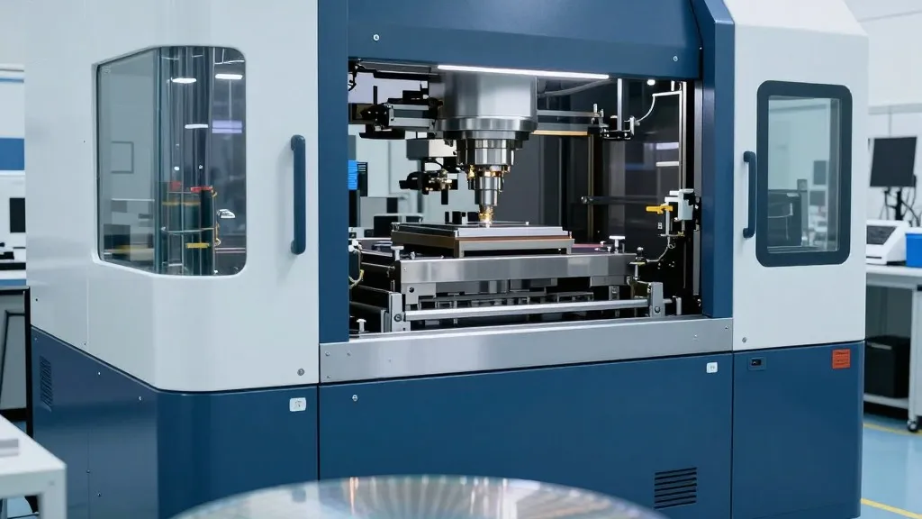
For families and businesses relying on the latest electronics, the supply chain remains a delicate balance. While export controls have kept the most advanced extreme ultraviolet lithography machines out of China, domestic chipmakers are still producing capable silicon. They achieve this by using older deep ultraviolet equipment and exposing critical layers multiple times. However, experts note that this workaround comes with significant trade-offs, including longer production times, higher defect rates, and increased costs for the final product.
The central issue is that ASML is the sole manufacturer of EUV machines, which use 13.5nm wavelength light to print the finest details on modern processors. Analysts estimate the technological gap between China and Western manufacturers in this area is at least five years. Despite this hurdle, Chinese firms have made unexpected progress. A teardown of Huawei's Mate 60 Pro revealed its processor was manufactured using a second-generation 7nm-class process without EUV. More recent analysis suggests further advancements toward 5nm density, though these processes still trail the leading technologies from TSMC and Samsung.
The technical method behind these advances is known as multiple patterning. Instead of printing a complex layer in a single pass, manufacturers break the design into simpler patterns and build the layer step by step. Chris Mack, co-founder and CTO of Fractilia, explains that industry wisdom suggests three exposures on a standard tool cost about the same as one EUV pass. However, when the process requires four masks, the older technology becomes more expensive than the advanced alternative.
Quality control is a major concern with this approach. Each new pattern must align perfectly with previous etchings, and more exposures lead to accumulated errors. Designers can add extra space around features to compensate, but this enlarges the chip size. A larger chip means fewer usable dies per wafer, which is a costly outcome when each wafer costs tens of thousands of dollars. As Mack puts it, manufacturers do not sell wafers, they sell the individual chips cut from them.
Memory production provides clear evidence of the efficiency gap. A recent report from Morgan Stanley estimated that Chinese DRAM maker CXMT produces only about one-third as many bits per wafer as its Western competitors. The bank described lithography access as a hard ceiling for development in this sector. Mack also cautioned that process labels like 5nm or 3nm have limited meaning on their own. He noted that while SMIC's newer process is progress, it remains significantly less scaled than established processes from major competitors.
There is still potential for growth with existing technology. Micron developed a recent DRAM generation without EUV by using tight process control and multiple patterning. Mack stated that this approach pushed the limits of the equipment farther than other memory makers had. Morgan Stanley believes CXMT's planned move to a similar technology for high-bandwidth memory is achievable without EUV. Researchers also expect advanced packaging to allow firms to use older tools for the latest DRAM generations by the end of the decade.
Even with these successes, the economic limits are becoming clear. Micron eventually switched to EUV for its latest DRAM, claiming more than a 30% increase in bit density per wafer compared to the previous generation. EUV has its own issues, such as stochastic effects that require higher exposure doses and added costs. Nevertheless, Mack expressed doubt that 3nm or 2nm nodes could be economically viable without the advanced lithography equipment.
Chinese chipmakers are not expected to stall, but they will likely accept larger dies, poorer yields, or longer manufacturing times. They can also increase overall capacity to offset these inefficiencies. Morgan Stanley projects that CXMT will lift its share of global DRAM bit supply from 14% in 2026 to 16% in 2028 through new factory construction. The bank also expects China's self-sufficiency in AI chips to rise from 42% in 2025 to 70% by 2030, even as persistent gaps remain in high-bandwidth memory and advanced software.
Source: Tom's Hardware